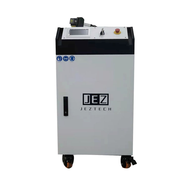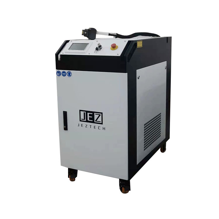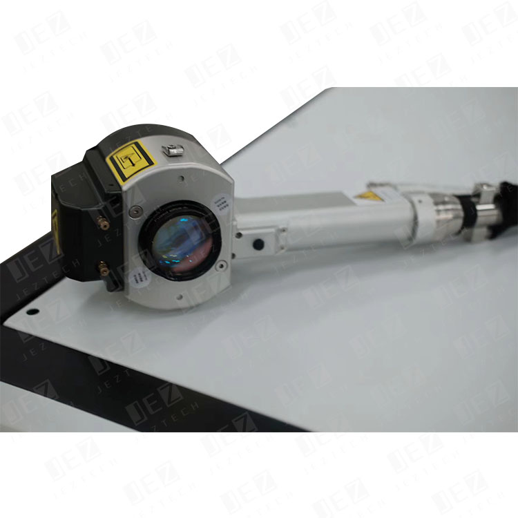
The Cupid Series Precision Laser Cleaning Machine has been garnering significant attention in various industries due to its innovative technology and versatile capabilities. In this comprehensive review, we delve into its performance specifically in the demanding field of semiconductor manufacturing, examining its key features and how they contribute to efficient, precise, and eco-friendly cleaning processes.

Key Features of the Cupid Laser Cleaning Machine
1. Large Laser Spot & High Single Pulse Energy Fiber Laser
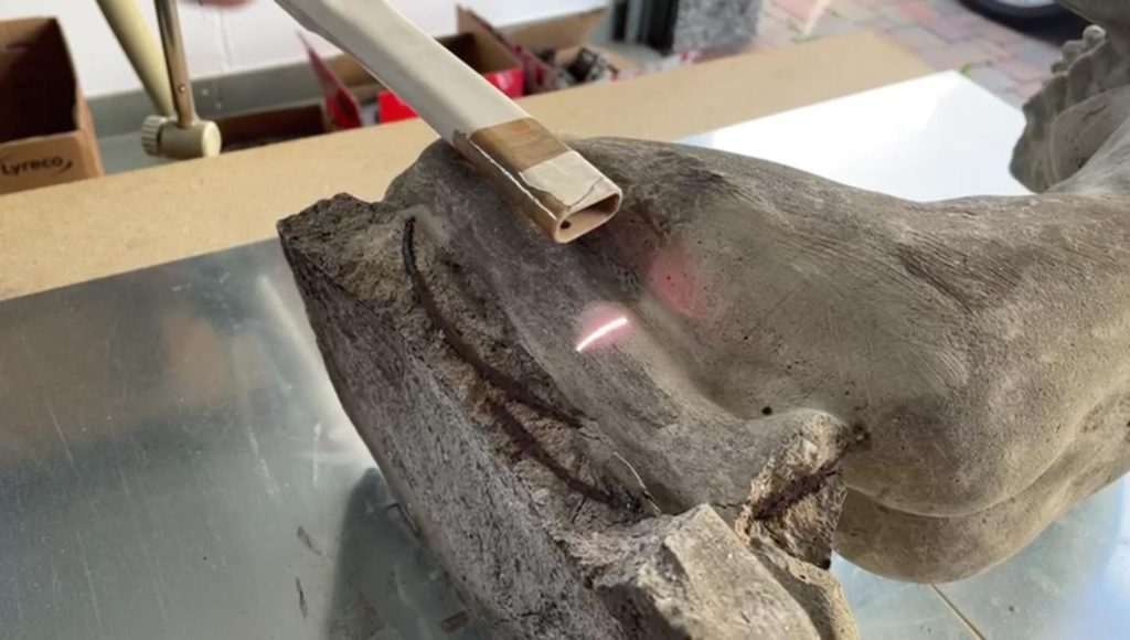
The Cupid laser cleaning machine boasts a large laser spot, enabling it to cover a wider area with each pass, significantly enhancing cleaning efficiency. Coupled with high single pulse energy, it delivers intense, focused cleaning power that effectively removes contaminants without damaging the underlying substrate material. This feature is crucial in semiconductor manufacturing, where precision and delicacy are paramount.
2. Simple Operation and Efficient Multiple Laser Cleaning Patterns
Designed for ease of use, the Cupid machine offers multiple laser cleaning patterns that can be tailored to specific applications. Its intuitive interface simplifies operation, enabling operators to quickly select and execute the most suitable cleaning pattern for each task. This flexibility ensures efficient cleaning of intricate semiconductor components, reducing downtime and increasing productivity.
3. Multiple Safety Operation Locks & Storable Working Parameters
Safety is paramount in any industrial setting, and the Cupid laser cleaning machine incorporates multiple safety operation locks to minimize the risk of accidents. Additionally, it can store multiple sets of working parameters, allowing users to conveniently retrieve and apply previously optimized settings for different cleaning tasks. This feature streamlines the work preparation process and ensures consistent, high-quality results across all semiconductor cleaning operations.
Benefits for Semiconductor Manufacturing
No Harm to Base Material
The precision of the Cupid laser cleaning technology ensures that only contaminants are removed, leaving the delicate semiconductor surfaces unscathed. This eliminates the risk of damage that can occur with traditional cleaning methods, preserving the integrity and performance of critical components.
Environmentally Friendly
By eliminating the need for chemicals and other media, the Cupid laser cleaning machine offers a green and environmentally friendly cleaning solution. This aligns perfectly with the sustainable practices increasingly adopted by the semiconductor industry, reducing waste and minimizing the environmental impact of manufacturing processes.
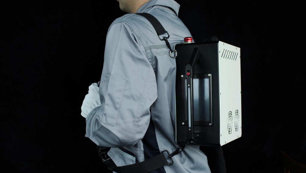
Compact Design for Mobile Operations
Highly integrated and occupying minimal space, the Cupid laser cleaning machine is ideal for mobile operations within semiconductor facilities. Its compact design facilitates easy transportation and setup, allowing for rapid response to cleaning needs across various production lines.
Application Scenarios in Semiconductor Manufacturing
While the Cupid laser cleaning machine has proven its worth in various industries, its application in semiconductor manufacturing is particularly noteworthy. It can be effectively utilized for:
– Wafer Cleaning: Removing particles, organic residues, and other contaminants from wafer surfaces during the manufacturing process.
– Packaging Cleaning: Ensuring cleanliness of packaging materials and components prior to assembly, preventing contamination during subsequent stages.
– Tool and Equipment Maintenance: Cleaning of production tools and equipment to maintain peak performance and extend their lifespan.
In conclusion, the Cupid Series Precision Laser Cleaning Machine has demonstrated exceptional performance in semiconductor manufacturing, offering a precise, efficient, and environmentally friendly solution for cleaning critical components. Its advanced features, including large laser spot size, high single pulse energy, and multiple safety operation locks, make it a valuable addition to any semiconductor manufacturing facility.